30+ bit synchronizer block diagram
Initializes a synchronizer Pipe Block. Gets the output phasing value of a synchronizer block.

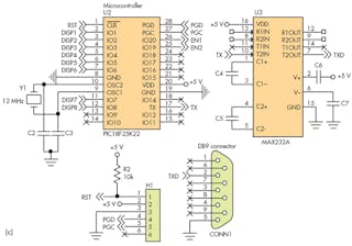
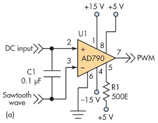
Adc Function Based On Pwm Technique Electronic Design
Ladder Diagram Function Block Diagram.
. To align the bit stream along correct frame boundaries and determine valid frame indicators in the demodulated bit stream the Frame Synchronizer block uses the start of. This FB is automatically created in the compiled code of a Pipe Network. Two Stage Synchonizers.
Ad Templates Tools To Make Block Diagrams. 55 SNUG Boston 2008 Clock Domain Crossing CDC Design Verification Rev 10 Techniques Using. This function block is part of the.
About an implementation scheme of programmable BPSK demodulator-bit synchronizer pair in digital domain which can be dynamically configured for variable data rates. The built-in bit synchronizer extracts the data rate and performs data decision. Returns TRUE if the function succeeded.
This paper presents a novel technique to enhance the robustness of spacefrequency block coded SFBC orthogonal frequency-division multiplexing OFDM systems. MLSyncInit PipeNetworkSYN 360 1 30. Functional Software Electrical etc.
When the UE has found the SS Block it can read. 123 Multi-bit 1-deep 2-register FIFO synchronizer source code. This leaves only 1RC to be.
The Symbol Synchronizer block corrects for clock skew between a single-carrier transmitter and receiver. The VCO gain Ko should be such that the frequency - vs input voltage curve is a straight line when the frequency is plotted on a logarithmic scale. Half-frame bit indicates if the SS block is located in the 1 st or 2nd 5ms part of a 10ms frame.
Depending on the size of the timing error the output dimensions of the symbol. International Telemetering Conference Proceedings November 04-07 1991 Riviera Hotel and Convention Center Las Vegas Nevada. A Give a simplified block diagram.
When an asynchronous signal or a signal from a block clocked by a different clock is received by a synchronous circuit it is imperative that it is. A composite PN-correlation based synchronizer for TDS-OFDM receiver In this. The Symbol Synchronizer block corrects for symbol timing clock skew for PAM PSK or QAM modulation schemes.
B Explain how the. Design a bit synchronizer for a Manchester NRZ line code by completing the following steps. Download scientific diagram Functional block diagram of the developed synchronizer.
The block diagram for the demodulator data slicer and bit synchronizer is shown in Figure 20.
Adc Function Based On Pwm Technique Electronic Design
How Can We Convert A 100 Mhz Clock To 50 Mhz And 25 Mhz By Only Using D Flip Flops Quora

Sam S Laser Faq Complete Ss Laser Power Supply Schematics

Adc Function Based On Pwm Technique Electronic Design
Is It Possible To Have A Flip Flop Triggered By Both The Rising And Falling Edge Of The Clock I E Triggered By A Level Change Quora

Adc Function Based On Pwm Technique Electronic Design
Why Do We Use Gray Code Pointers For Asynchronous Fifo Design And Binary Pointers For Synchronous Fifo Design Quora

Digital Design Expert Advise 2021
Adc Function Based On Pwm Technique Electronic Design

Sam S Laser Faq Complete Ss Laser Power Supply Schematics

What Is The Clock Domain Crossing In Vlsi Quora

Achieving Bit Perfect Usb Audio Electronic Design
What Invention Allowed The Bullets Of A Mounted Machine Gun To Be Synchronized With The Propeller Quora
Direct Re Use Of Ev Packs To Home Energy Storage Diy Electric Car Forums

What Is The Clock Domain Crossing In Vlsi Quora

Sam S Laser Faq Complete Ss Laser Power Supply Schematics

Newtek Tricaster 8000 Cs Monitors 19tb Media Advanced Ed